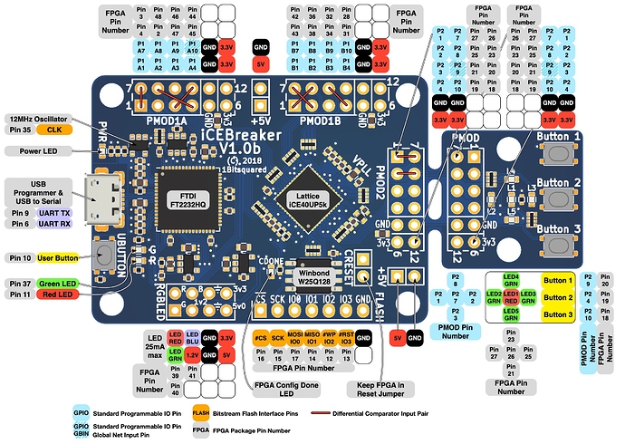
Why are jumpers shown on the Icebreaker board diagrams at PMOD1A, PMOD1B, and PMOD2?
Hi @otto9C9otto,
Welcome to the forum.
I assume you refer to the pads between the GND and 3v3 pins of the Pmod connectors. These are not jumpers, they are optional footprints for decoupling capacitors. If you have a Pmod that does not have good decoupling, or you are trying to improve supply stability you can solder 10uF 0603 ceramic capacitors on these footprints.
We have designed in those capacitors and decided not to populate them, as they are not needed in most cases. That said as a user you might decide to populate them on your iCEBreaker.
I hope it helps.
Cheers,
Piotr
I am still puzzled because, for instance, PMOD1A is jumpered from pin 1 to pin 7, which corresponds to the FPGA pins 3 and 4. Also jumpered is PMOD1A pin 3 to pin 10, corresponding to FPGA pins 47 and 44. Also jumpered is PMOD1A pins 4 and pin 8, which is FPGA pins 45 and 48.
On PMOD1B, pin 1 is jumpered to pin 8, which is FPGA pins 43 and 36, Also pin 2 is jumpered to pin 7, which is FPGA pins 38 and 42. Also pin 4 is jumpered to pin 9, which is FPGA pins 31 and 32.
On PMOD2 pin 1 is jumpered to pin 7, which is FPGA pins 27 and 26. Also pin 2 is jumpered to pin 8, which is FPGA pins 25 and 23.
For reference here is the diagram. So that we are talking about the same thing.
Are you referring to the red lines between the pins of the Pmods? Those are not jumpers, these are the pins that form a DiffPair. This means you can use them together to implement a differential-pair input.
The red lines have a description at the bottom of the diagram.
Cheers,
Piotr
OK, now I understand. Thanks.
