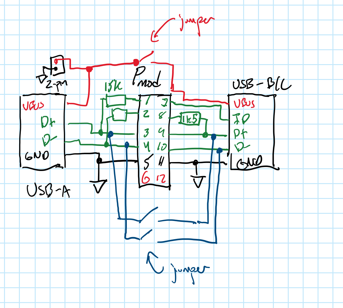
So I ended up nerdsniping myself into building a calculator for the diode PU/PD circuitry (it’s on JSFiddle so you can also view/edit source code).
I kinda wanted to integrate the circuit it assumes, into the page, so it’s overall clearer about what’s going on, but I wasn’t sure about how to proceed with that (suggestions welcome).
It makes these assumptions:
- one side pulls up, the other side pulls down, on the same line
- any cable resistance between the two sides, or input impedance connected to that line, is negligible
- therefore, the pull-up and pull-down combine to form a voltage divider, producing the “idle voltage”
I’ve more or less confirmed the voltage divider aspect for the USB D-/D+ case, thanks to this paragraph in the “Resistor ECN” document in the USB 2.0 spec:
These alternative means must produce an idle voltage (VIHZ) on D- or D+ of between 2.7 V and 3.6 V when terminated with a pull-down resistance of 15 kΩ±5% to ground.
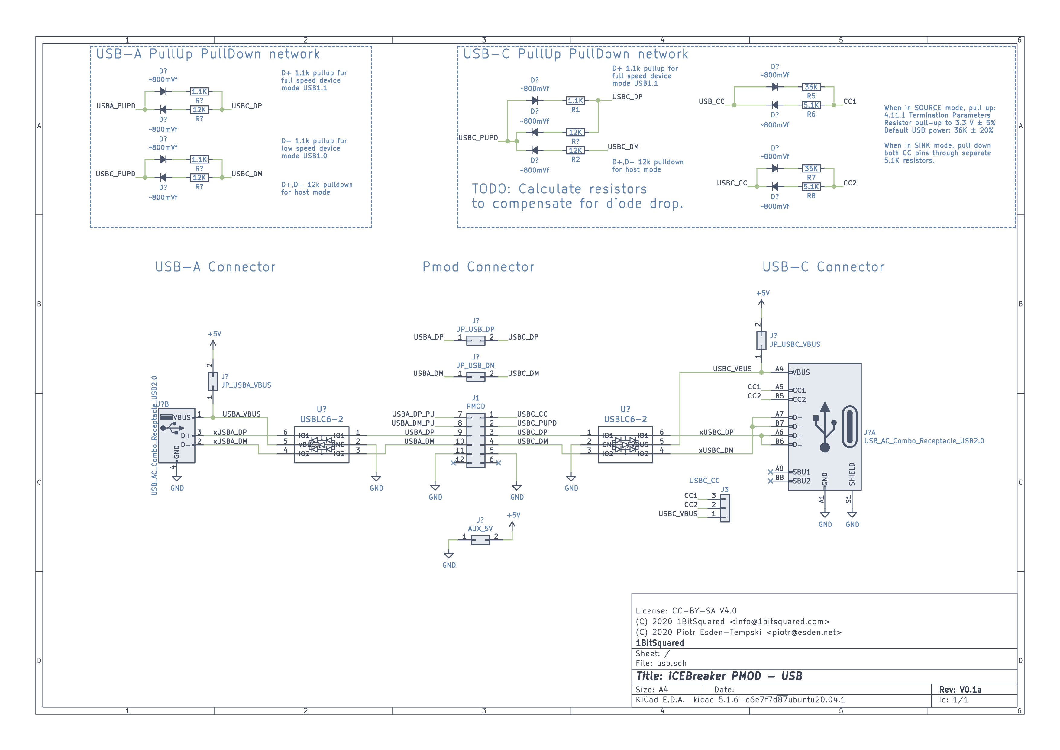
Relevant (to this pmod) standard values:
|
D-/D+ |
CC |
| Rpull-up |
1.5kΩ |
36kΩ |
| Rpull-down |
15kΩ |
5.1kΩ |
| Vidle |
3V |
0.409V |
Trying to replicate the standard Vidle isn’t easy with a diode drop, on the side closest to either 0V (down for CC) or 3.3V (up for D-/D+). In fact, a 800mV diode in a pull-up circuit will drop from 3.3V to 2.5V, which is already below the 2.7V minimum in the USB spec (for D-/D+ idle voltage).
To be clear, I’m not saying it won’t work, just that we might want to avoid diodes with a large forward drop in this kind of circuit, for maximum compatibility.
If 220mV diodes (Schottky?) are an option, they would allow reproducing the exact Vidle, with the following resistor values (warning: I haven’t looked at current or dissipated power at all):
|
D-/D+ |
CC |
| Rpull-up |
0.4kΩ |
33.26kΩ |
| Rpull-down |
13.9kΩ |
2.36kΩ |
It’s still possible to use 800mV diodes for D-/D+ pull-down or CC pull-up (which have more voltage margin), I suppose it mostly depends on price and other characteristics I haven’t looked at.
If the 400Ω pull-up for D-/D+ seems a bit too low, it can be increased to any value below 2kΩ without going out of spec (when using a 220mV diode, that is - diodes with a larger drop require smaller resistors).
EDIT: it’s definitely too low, @tnt pointed out on Discord that I’m not accounting for the output driver impedance, and its ability to pull D-/D+ down to a logic low (below 0.3V for low/full-speed).
I’ll try to get that in somehow, probably by finding the max output impedance that would (barely) work for the standard PU/PD values and then compute what logic low/high voltage such a driver would be able to produce.
Preliminary testing shows that one needs at least 1.4kΩ pull-up (for 220mV diode drop), 400Ω is nowhere near enough to allow worst-case output driver to pull a logic low (best-case is plausible, based on the spec, but we want it to work with all spec-compliant hardware not just a small subset).
And I haven’t looked at all at the requirements on the CC lines.