I have this idea in mind and was hoping people here could pick holes in it or flag any risks, considering I can’t run my designs on a board yet and even if it does work, I want to be certain it’s reliable:
12mhz in to SB_PLL40_2F_PAD
25mhz out to GLOBALA
12.5mhz out to GLOBALB using GENCLK_HALF
The 2F_PAD seems to support this from looking at existing designs.
Can I assume that the 25mhz and 12.5mhz are in phase or close enough to it, such that the posedge of the half-speed clock aligns with the posedge of every other full-speed clock? Or do I need to do the whole CDC thing in this case? Any input appreciated
They won’t drift, but they’re definitely not aligned. There is a couple of nanosecond difference between the two because the A output goes through more output muxes.
But what you can do is use the negative edge of the fast clock to give you more margin. But you definitely want to go from register to register without any logic in between. No need for the dual capture reg if you ensure your delays are good and provide margin, unfortunately nextpnr doesn’t support such constraints so you need to check manually or instanciate FFs manually and place them manually.
Thanks, really helps to know these details. The idea of using the negedge of the fast clock is interesting. For my design then, there could be a module between the slow CPU and the fast peripheral that it’s writing to. Something like:
posedge slowclk: clock FFs containing data/addr/whatever from slow cpu (stage 1)
20ns later: negedge fastclk: clock FFs from stage 1 to stage 2
20ns later: posedge fastclk: clock FFs from stage 2 to stage 3 (not necessary?)
Then wire stage 3 to the input of the fast peripheral, which then has stable data as if it came from any other posedge-fastclk clocked FF. The negedge implies I need to worry about the duty cycle of the clock coming out of the PLL but should be fine according to the data sheet?
Right now every FF in my design is clocked on posedge-slowclk but the fast peripheral in this scenario is a video controller so if I want the full resolution mode to work, have to double that pixel clock. I suppose adding this intermediate module would allow me to reuse the rest of the design.
I’ve never tried manual placement. Still worth doing with the module described above? I’ll start reading the docs for it as it’s good to know and I may as well have a go with this when the time comes.
Step 3 is not needed, the tool will analyze the path correclty from the FF of step 2 to any further logic in the 25 MHz domain. Note that of course since you only have a clock cycle there you might find you don’t meet timing … so try to keep your “input” combinatorial path short.
In the timing report nextpnr will output what the max delay from posedge slowclk -> nededge fastclock is. There is no way to constrain it and the tool will not optimize for it, but you should at least check yourself to make sure that this delay is less than ~ 15 ns (20 ns cycle - 5ns of ‘skew’ betweeen clock) Being from FFs to FFs, it should pretty much meet that no problem all the time but if something break, check it
You shouldn’t need to go to manual placement for such slow clock speeds, even the “randomized” nextpnr placement should be fine. In 15ns you can pretty much cross from one side of the FPGA to another …
Tried the approach described here and works great, no weird surprises. Only extra bit of work to do was expected: write enables and any other control signals with side effects have to be masked out in the second cycle or else it’ll try writing video memory twice, poking weird values into the scrolling layer offsets etc. I was hoping that’s all that was needed.
Just had to add an extra constraint and then… ctx.addClock("testvdp.clk", 33.716)
Info: Max frequency for clock           'cpu_clk': 17.68 MHz (PASS at 16.86 MHz)
Info: Max frequency for clock 'vga_clk$SB_IO_OUT': 43.87 MHz (PASS at 33.72 MHz)

Info: Max delay <async>                   -> posedge cpu_clk          : 4.65 ns
Info: Max delay posedge cpu_clk           -> <async>                  : 5.64 ns
Info: Max delay posedge cpu_clk           -> posedge vga_clk$SB_IO_OUT: 11.14 ns
Info: Max delay posedge cpu_clk           -> negedge vga_clk$SB_IO_OUT: 5.62 ns
Info: Max delay posedge vga_clk$SB_IO_OUT -> <async>                  : 6.29 ns
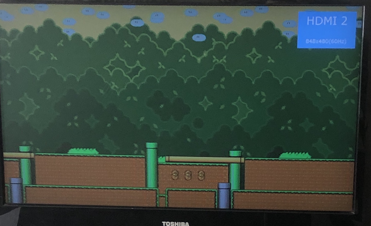
Looks like there’s plenty of headroom assuming the posedge -> negedge delay is where the described fastclk -> slowclk FF load is happening. I bumped the PLL and the VGA timings from 640x480 to 848x480 since the budget is there and it looks nicer on a 16:9 TV. Conveniently it also bumps the CPU clock closer to fmax. Huge difference it makes though, no more super blocky pixels and uses about the same slices as the 320x240 single-clock approach.