In this thread I want to discuss hardware designs and toolchains that could turn the Colorlight 5A-75B LED receiver card [1] into a usable FPGA development platform. In the start of 2020 people on twitter discussed the reverse engineering of this board which resulted in a GitHub repo with pictures, pinouts and example code.
Features
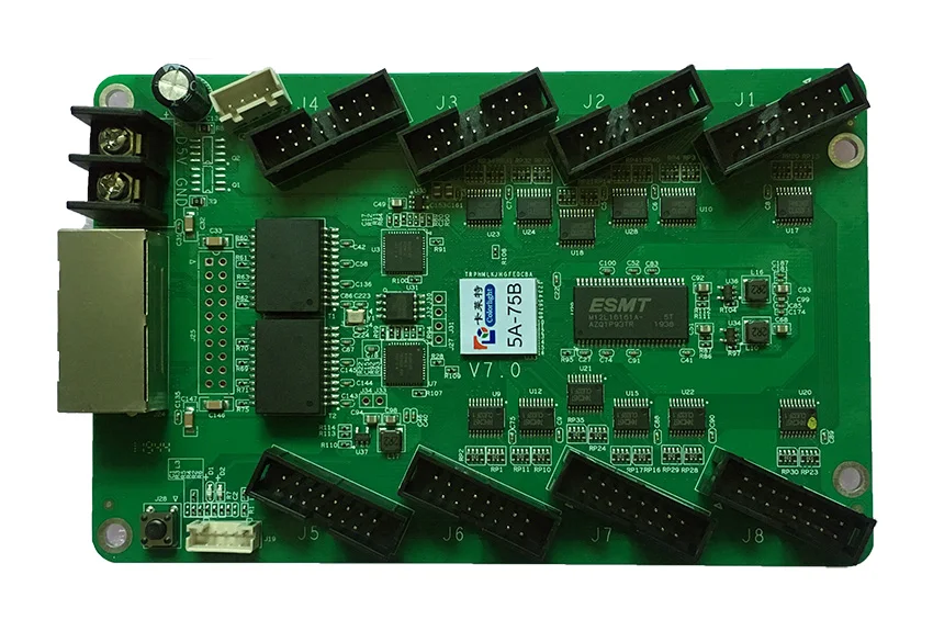
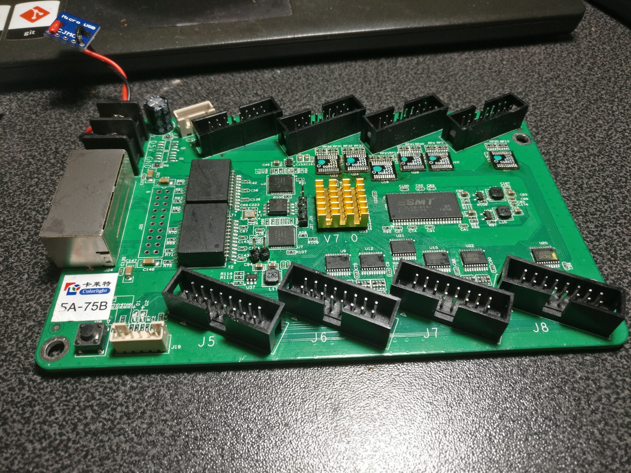
The Colorlight 5A-75B is an interesting target because of its low price [2], DSP and SERDES capabilities, high IO count and pre-installed preipherals:
- 1 25Q16 serial PROM for FPGA configuration
- 2 1M x 16bit SDRAMs
- 2 1Gb Ethernet PHYs
Enable Input
TL;DR without modding the board, the pins are output only.
The problem with this board is that all pins of the HUB75 connectors are connected to the outputs of signal buffer, meaning that they are all output only. If one were to lift the direction pin of the buffers and turn them into an input, they would output +5V to the FPGA which would kill it. Do not attempt!
My current approach [3] is to desolder the buffer ICs and replace them with PCBs that simply connects each input to the corresponding output.
[img1]
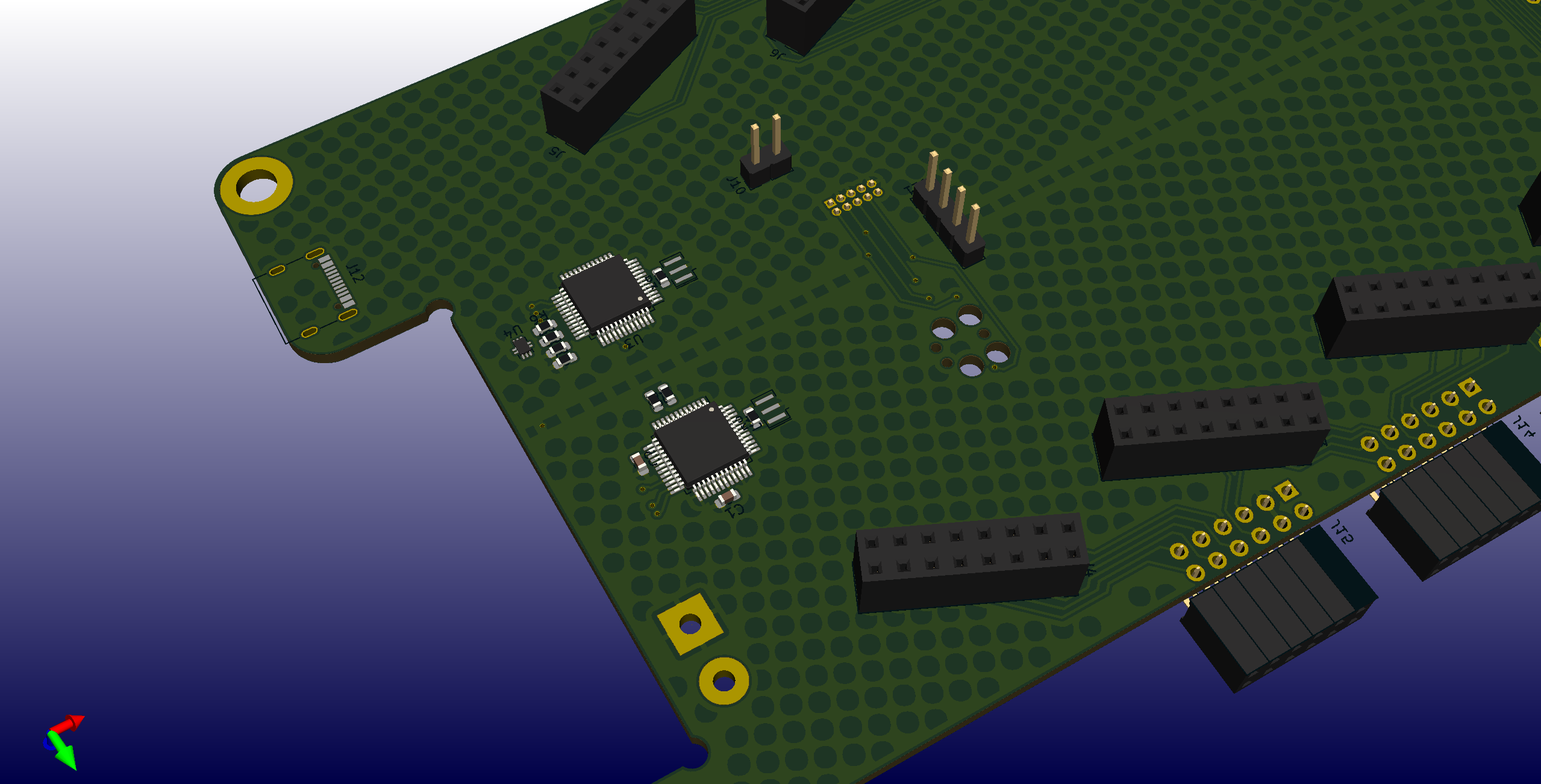
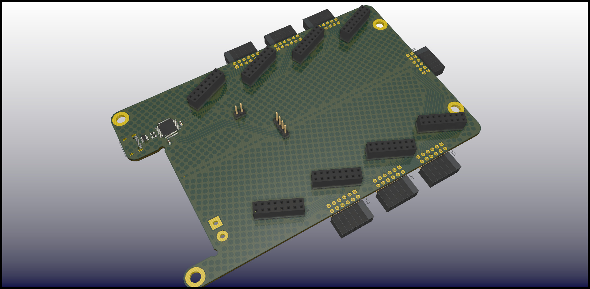
Hardware Design
[img2]
As a basis for hardware designs I measures the positions and angles of the connectors on the board and transferred them to a KiCAD PCB layout.
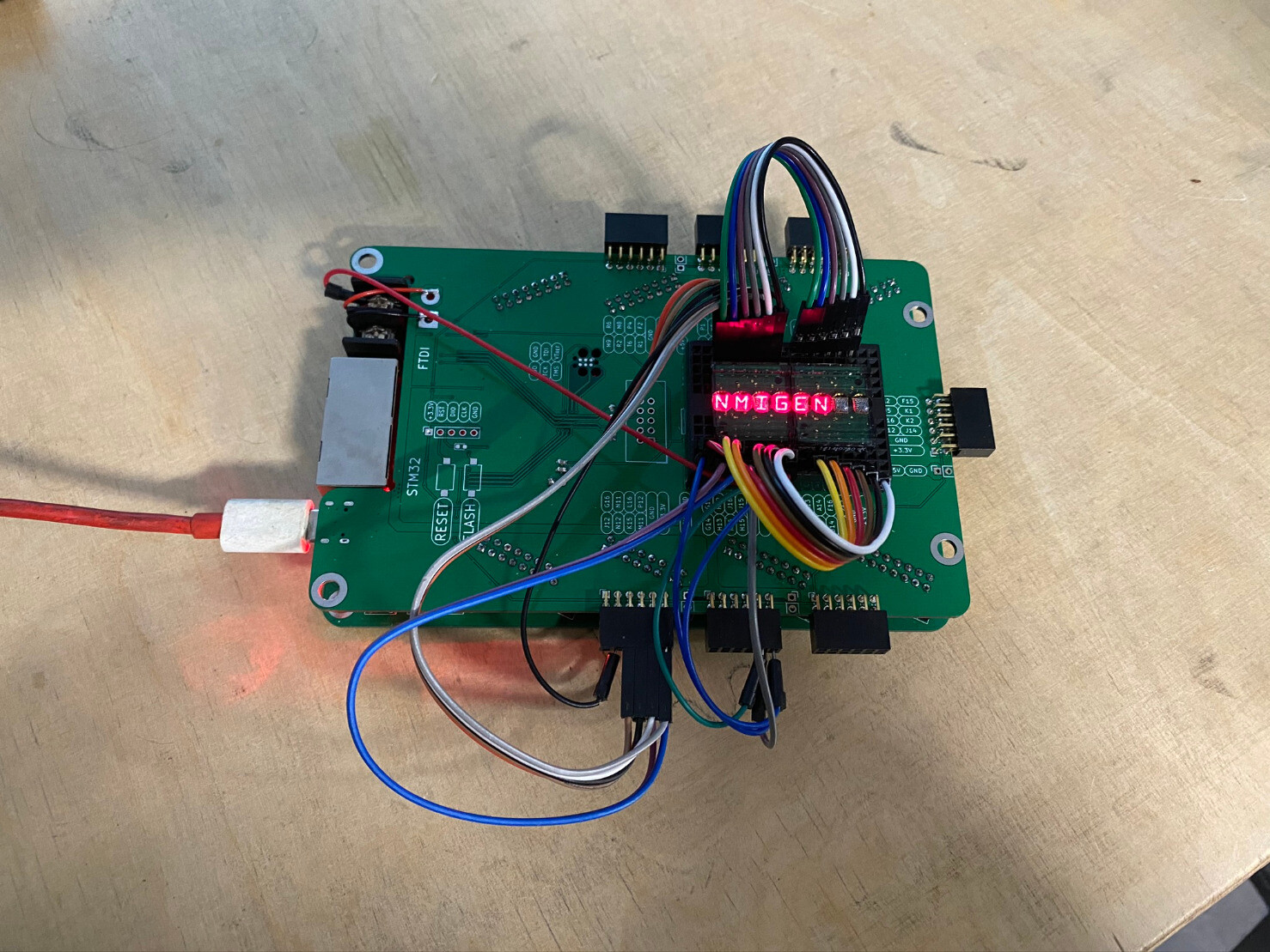
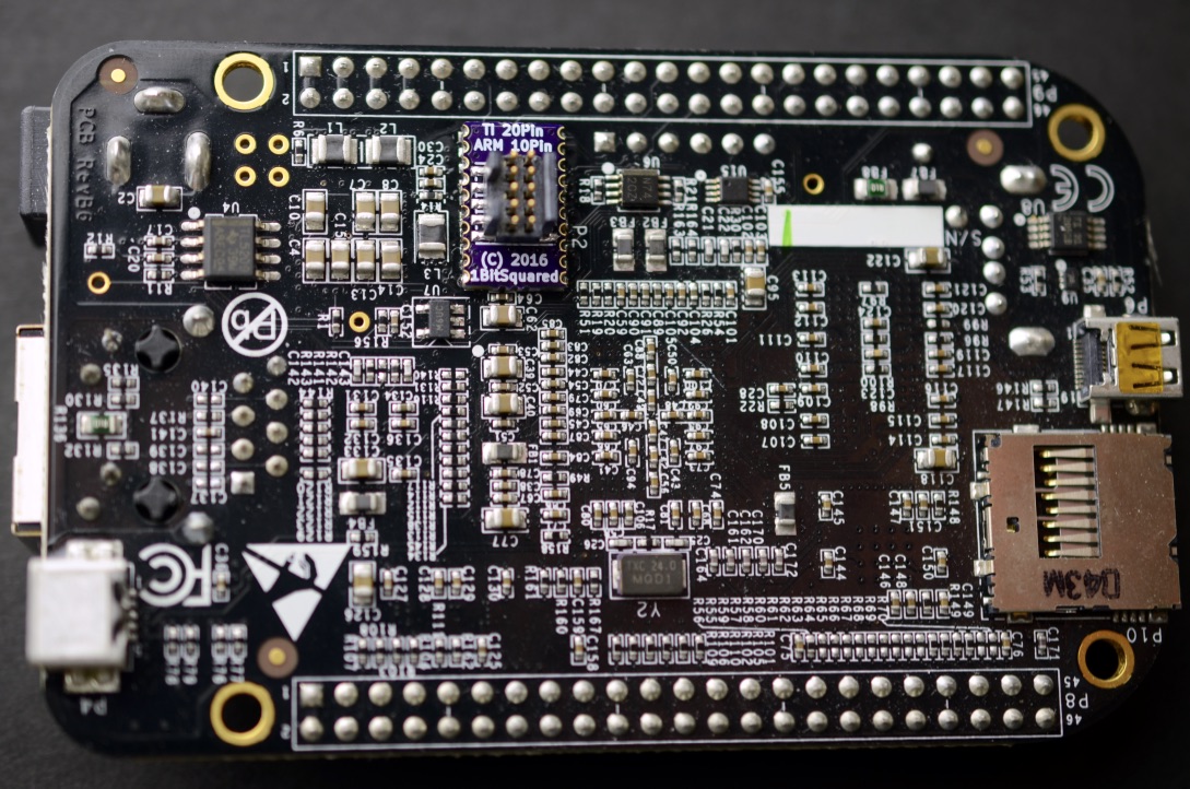
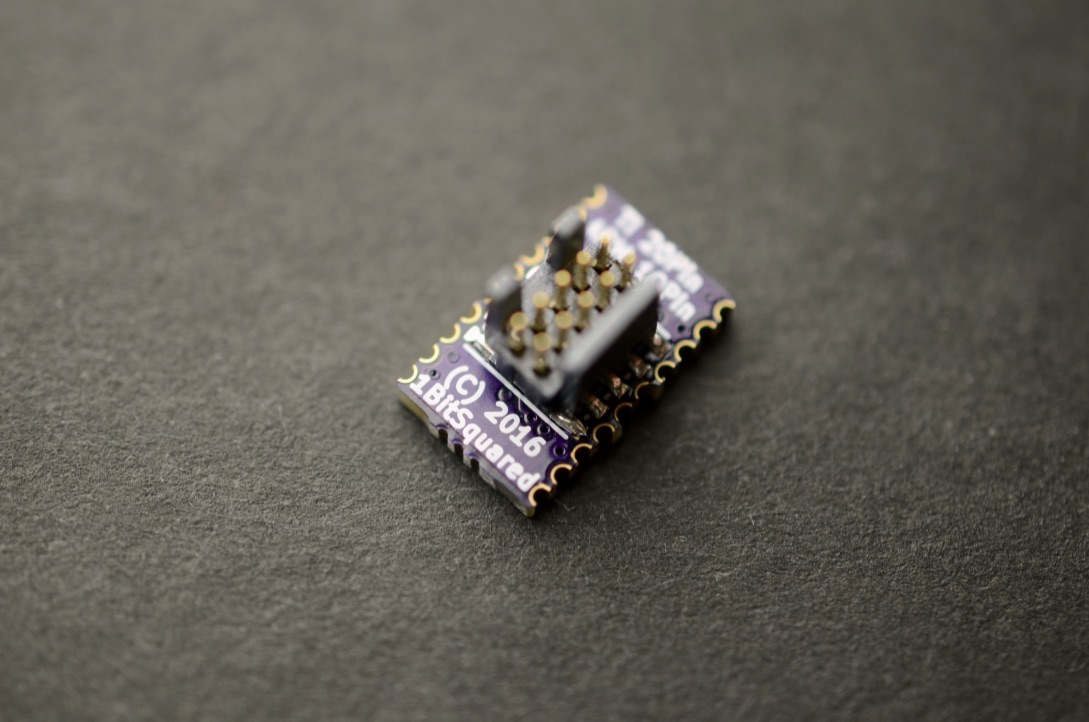
Programmer
Since iceprog is a simple programming tool for FTDI-based Lattice iCE programmers, I added a FT2232H for programming (and maybe even debugging ?) capabilities.
It is directly connected to the JTAG interface of the FPGA. Additionally we could connect two pins for UART.
Connectors
There are 56 individual signals available from the eight HUB75 connectors. I regrouped them into seven Pmod connectors. The ones on the side are spaced in a way that this board provides two double Pmods and three single Pmods.
Another Idea is to design a board for human interface devices. With connectors for video, audio and input devices (e.g. USB, HDMI, VGA, PS/2, LVDS etc.). This may require measuring delay in signals and tuning the length of the traces.
Toolchain
There already is a LiteX platform file [4] for the Colorlight. LiteX is written in Migen, but I would like to use nMigen.
Currently I’m trying to write a nMigen board file based on the LiteX Migen file.
If someone is interested, I can clean up and upload the CAD files to GitHub 
As a first time poster, I can only add two links and one image  I add the other links and imaged in the thread.
 open source USB-JTAG implementations? Maybe something with and STM32? To be viable it would need to be about as cheap as the FTDI, which is ~7€